


Product Info
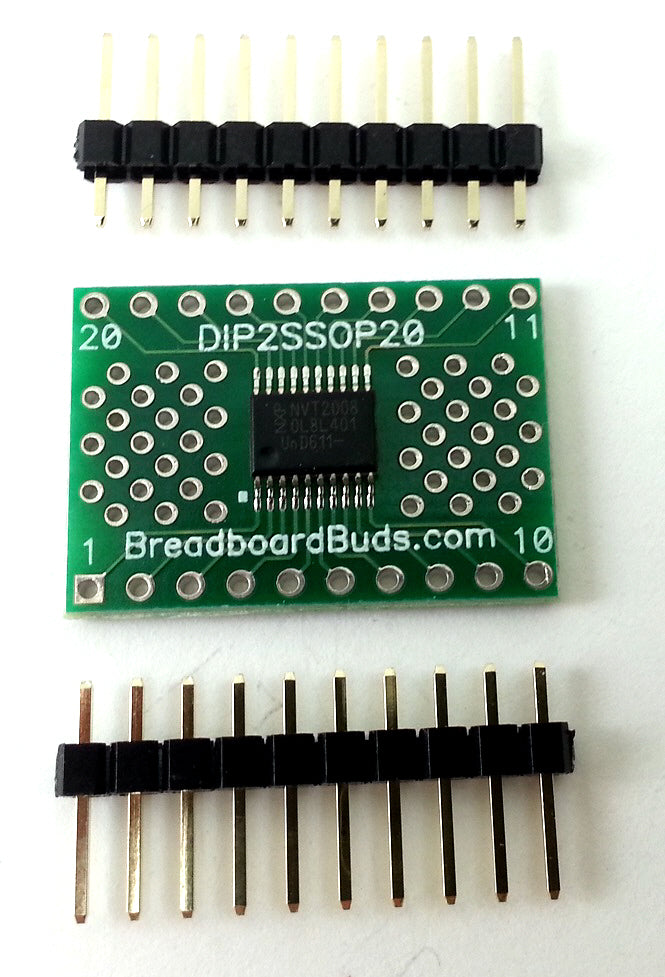
This breakout board provides eight bi-directional voltage level translation channels, ideal for such things as SPI (e.g. SD card interface, MP3 chip interface) and port interfacing. The 20-pin TSSOP level shifter chip is mounted on a carrier and fits a standard 0.6" wide DIP footprint. A strip of 20 square pins is provided, but not soldered into place.
Features:
- enables low-voltage peripherals to be used in 3V or 5V systems
- also supports voltage translation between other levels (1.2V/3V/5V)
- solderless breadboard friendly design
- strip of 20 square pins is provided, but not soldered into place
- can be plugged into a standard 0.6" wide DIP socket
- end-to-end stackable
- based on the NXP NVT2008:
- 8-Bit Bidirectional Voltage-Level Translator
- Auto Direction Sensing
- +/-15-kV ESD Protection
- up to 33 Mbps throughput, depending on voltage differential
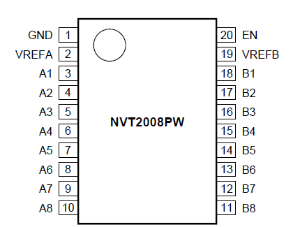
- direct one-to-one pin-numbering
Details
This 8-bit non-inverting translator uses two separate configurable power-supply rails. The A port is designed to track VCCA. VCCA accepts any supply voltage from 1.0 V to 3.6 V. The B port is designed to track VCCB. VCCB accepts any supply voltage from 1.8 V to 5.5 V. This allows for universal low-voltage bidirectional translation between any of the 1.0-V, 1.5-V, 1.8-V, 2.5-V, 3.3-V, and 5-V voltage nodes. VCCA should not exceed VCCB.
When the EN input is low, all outputs are placed in the high-impedance state.
All channels have the same electrical characteristics and there is minimal deviation from one output to another in voltage or propagation delay. This is a benefit over discrete transistor voltage translation solutions, since the fabrication of the switch is symmetrical. The translator provides excellent ESD protection to lower voltage devices, and at the same time protects less ESD-resistant devices.